Description
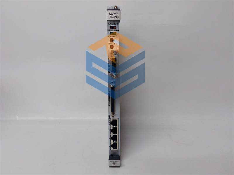
MVME162-201
Programming Model
This section defines the programming model for the control and status
registers (CSRs) in the MCECC pair. The base address of the CSRs is hard
coded to the address $FFF43000 for the MCECC pair on the first
mezzanine board and $FFF43100 for the MCECC pair on the second
mezzanine board. The CSRs for the two MCECCs appear at the same
address, (one on D16-D31, the other on D00-D15).
Hardware automatically duplicates the values that are written to the CSRs
in the upper MCECC (the one that connects to D16-D31) to the lower
MCECC (the one that connects to D0-D15). Hence Software only needs
to write to the control registers in the upper MCECC. This duplicating
function can be disabled by software for test purposes.
A Note on the “Differences with MEMC040” information
in this section
In some other MVME product families, the MCECC corresponds to a
parity memory controller, the MEMC040, with which it shares a group of
similarly-defined registers. For reference purposes, differences between
these registers are briefly documented in this section as described below,
but the MEMC040 is not used on any MVME162LX boards.
The first eight registers of the MCECC pair are those whose register map
was made to look as similar as possible to the map for the same eight
registers contained in the MEMC040. Where there are differences, they
are noted. The remaining 18 registers contain functions unique to the
MCECC pair.
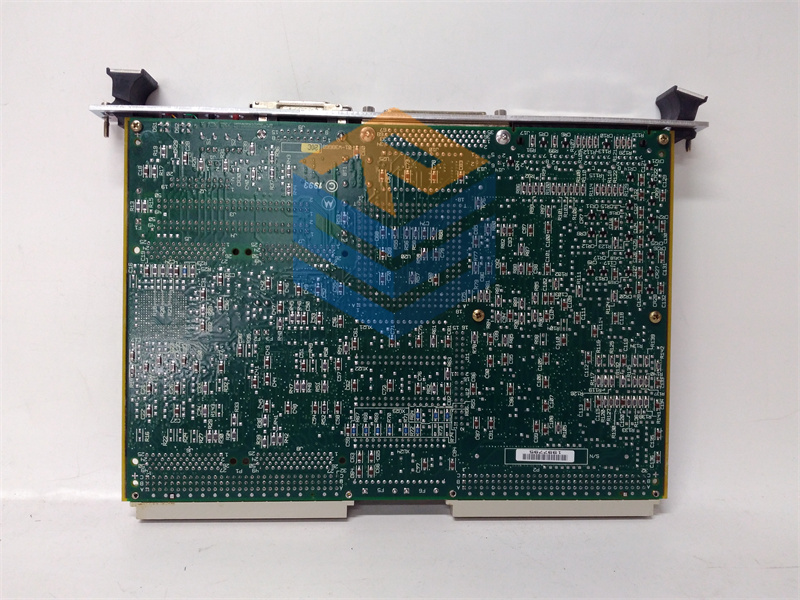
MVME162-010A
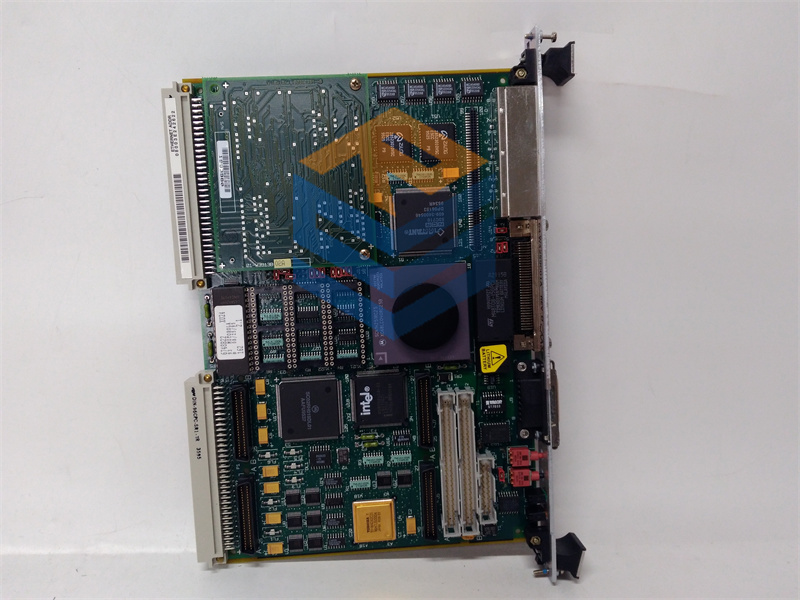
MVME162-201
All prices listed on the official website are subject to confirmation by contact: Wu Jiedong (manager).
Our product: brand new original packaging
Our warranty: All new or repaired parts have a 12 month warranty period beginning
Our payment: 100% telegraphic transfer of inventory items before shipment, conditions can be proposed!
If you have any downtime spare parts that you cannot find, please feel free to call or use email to contact me. If there are issues that the product cannot solve, please contact me. Product prices can be negotiated. Please do not consider contacting me!

