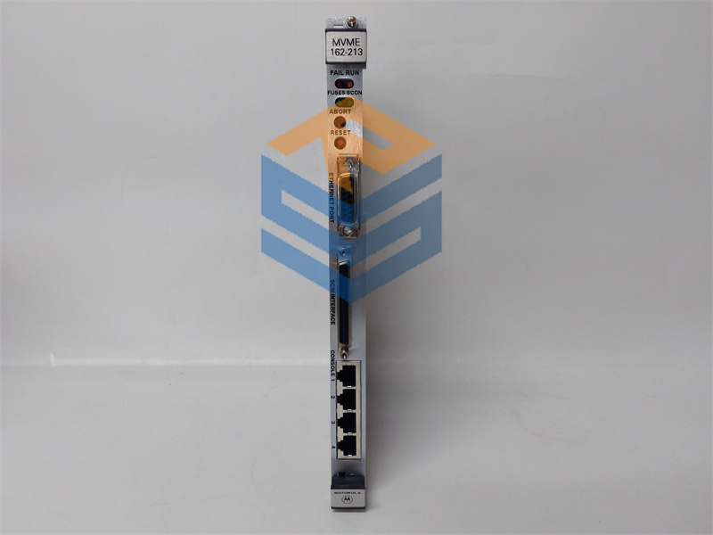
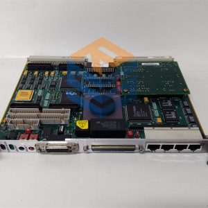
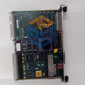
MVME162-453 modular

MVME162-453

The EPROM and Flash are sized by the MCchip ASIC from an

8-bit private bus to the 32-bit MPU local bus. Because the

device size is less than the allocated memory map for some

entries, the device contents repeat for those entries.

If jumper GPIO3 is installed, the Flash device is accessed. If

GPIO3 is not installed, the EPROM is accessed.

The Flash and EPROM are sized by the MCchip ASIC from an

8-bit private bus to the 32-bit MPU local bus. Because the

device size is less than the allocated memory map for some

entries, the device contents repeat for those entries.

If jumper GPIO3 is installed, the PROM device is accessed. If

GPIO3 is not installed, the Flash is accessed.

These areas are not decoded unless one of the programmable

decoders are initialized to decode this space. If they are not

decoded, an access to this address range will generate a local

bus timeout. The local bus timer must be enabled.

Category:
Email: Jiedong@sxrszdh.com
Phone: +86 15340683922
Sales:Wu Jiedong
All prices listed on the official website are subject to confirmation by contact: Wu Jiedong (manager).
Our product: brand new original packaging
Our payment: 100% telegraphic transfer of inventory items before shipment, conditions can be proposed!
If you have any downtime spare parts that you cannot find, please feel free to call or use email to contact me. If there are issues that the product cannot solve, please contact me. Product prices can be negotiated. Please do not consider contacting me!

Description

MVME162-453

Memory Maps
There are two points of view for memory maps:
❏ The mapping of all resources as viewed by local bus masters (local bus
memory map)
❏ The mapping of onboard resources as viewed by VMEbus masters
(VMEbus memory map)
Local Bus Memory Map
The local bus memory map is split into different address spaces by the
Transfer Type (TT) signals. The local resources respond to the normal access
and interrupt acknowledge codes.
Normal Address Range
The memory map of devices that respond to the normal address range is
shown in the following tables. The normal address range is defined by the TT
signals on the local bus. For the MVME162, transfer types 0, 1, and 2 define the
normal address range. Table 3-1 defines the entire map ($00000000 to
$FFFFFFFF). Many areas of the map are user-programmable, and suggested
uses are shown in the table. The cache inhibit function is programmable in the
MC68xx040 MMU. The onboard I/O space must be marked ‘‘cache inhibit’’
and serialized in its page table. Table 3-2 further defines the map for the local
I/O devices
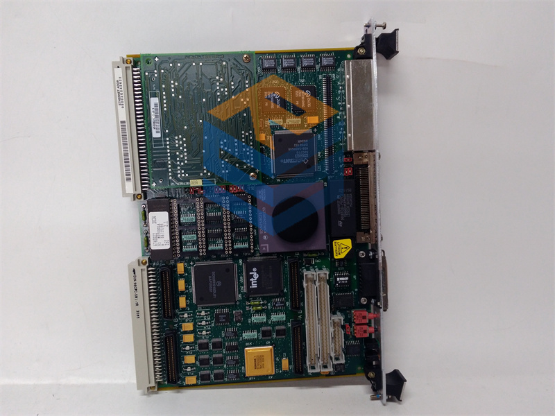
MVME162-412

MVME162-412
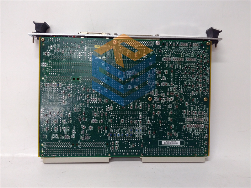
MVME162-412

MVME162-412

MVME162-453

MVME162-453

Email: Jiedong@sxrszdh.com
Phone: +86 15340683922
Sales:Wu Jiedong
Our products are guaranteed for 1 year, with new and original production stopped and imported spare parts.
All prices listed on the official website are subject to confirmation by contact: Wu Jiedong (manager).
Our product: brand new original packaging
Our warranty: All new or repaired parts have a 12 month warranty period beginning
Our payment: 100% telegraphic transfer of inventory items before shipment, conditions can be proposed!
If you have any downtime spare parts that you cannot find, please feel free to call or use email to contact me. If there are issues that the product cannot solve, please contact me. Product prices can be negotiated. Please do not consider contacting me!